


MTW European Type Trapezium Mill
Input size:30-50mm
Capacity: 3-50t/h
LM Vertical Roller Mill
Input size:38-65mm
Capacity: 13-70t/h
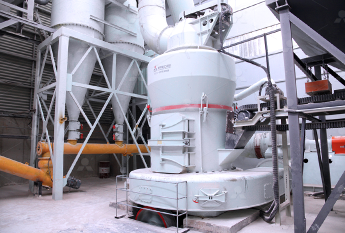
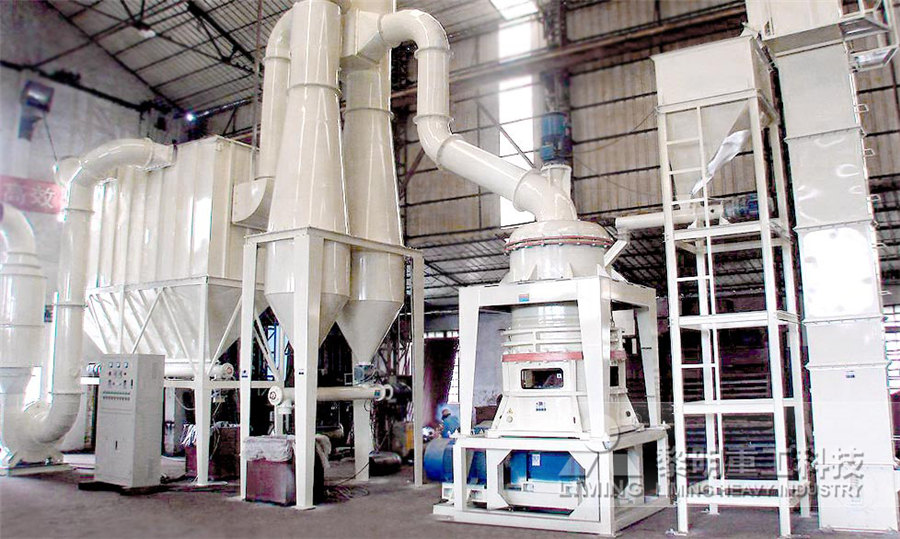
Raymond Mill
Input size:20-30mm
Capacity: 0.8-9.5t/h
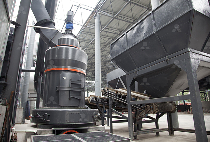
Sand powder vertical mill
Input size:30-55mm
Capacity: 30-900t/h
LUM series superfine vertical roller grinding mill
Input size:10-20mm
Capacity: 5-18t/h
MW Micro Powder Mill
Input size:≤20mm
Capacity: 0.5-12t/h

LM Vertical Slag Mill
Input size:38-65mm
Capacity: 7-100t/h
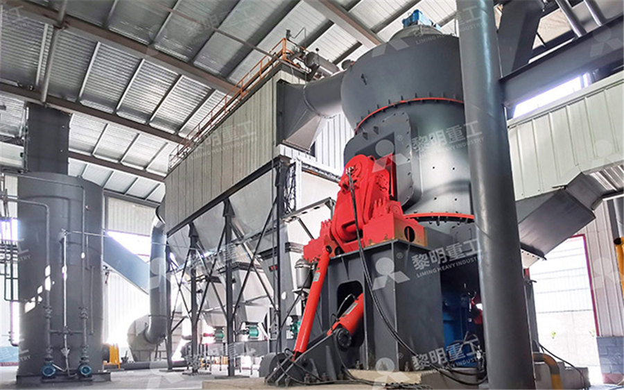
LM Vertical Coal Mill
Input size:≤50mm
Capacity: 5-100t/h
TGM Trapezium Mill
Input size:25-40mm
Capacity: 3-36t/h
MB5X Pendulum Roller Grinding Mill
Input size:25-55mm
Capacity: 4-100t/h
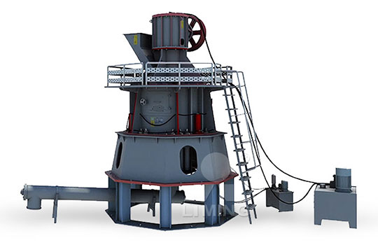
Straight-Through Centrifugal Mill
Input size:30-40mm
Capacity: 15-45t/h
Harm to the body of working in a monocrystalline silicon factory

[PDF] Defects in Monocrystalline Silicon Semantic Scholar
The aggregation of instrinsic point defects (vacancies and Si interstitials) in monocrystalline silicon has a major impact on the functioning of electronic devices2017年1月1日 The aggregation of instrinsic point defects (vacancies and Si interstitials) in monocrystalline silicon has a major impact on the functioning of electronic devices While agglomeration of vacancies results in the formation Defects in Monocrystalline Silicon SpringerLink2017年1月1日 The aggregation of instrinsic point defects (vacancies and Si interstitials) in monocrystalline silicon has a major impact on the functioning of electronic devicesDefects in Monocrystalline Silicon Request PDF ResearchGate2014年11月30日 However, the intensive electrical spark between a wire electrode and silicon can cause damage to the cut surface and subsurface in micro and nanoscale aspects This Surface characteristics and damage of monocrystalline silicon
Silicon Materials SpringerLink
2023年11月28日 The material possesses the advantages of perfect crystal lattice, less defects and impurities, and is the basic material for IC industry There are two kinds of monocrystalline 2023年9月1日 Herein, this study employs nanoscratch tests to explore the anisotropy dependence on material removal and deformation mechanism for monocrystal silicon Influence of anisotropy on material removal and deformation 2021年4月9日 In this study, the slight damages, ie protrusive hillocks resulting from nanoscratching on monocrystalline silicon surface, was thermally annealed in vacuum for Repairing slight damages on monocrystalline silicon surface by 2019年6月10日 With largescale molecular dynamics, we investigate displacement cascades in monocrystalline silicon with regard to the effects of temperature, strain, and primary knockon Displacement Cascades in Monocrystalline Silicon: Effects of
.jpg)
General Molecular Dynamics Approach to Understand the
2021年7月30日 The present paper aims to reveal the mechanical anisotropy of monocrystalline silicon under the nanoscale effects of point defects and provides a reference for the 2024年10月1日 The simulation results reveal that temperature closely correlates with plastic deformation, indentation force, internal stress, and defects in nanoindentation This study The effect of temperature on monocrystalline Si nanoindentation 2017年12月22日 Effect of abrasive shape on the threebody abrasion behaviors of monocrystalline silicon was investigated by Molecular dynamics modelling The axial ratio of abrasive particle was varied from 100 (PDF) Influence of Abrasive Shape on the Abrasion and 2022年1月1日 To solve seeding failures due to the misjudgment caused by manual observation in the traditional melting process of Czochralski (CZ) monocrystalline silicon, a method for predicting the melting (PDF) The CNN Deep LearningBased Melting Process

Monocrystalline silicon solar cells applied in
2012年7月1日 Purpose: The aim of the paper is to fabricate the monocrystalline silicon solar cells using the conventional technology by means of screen printing process and to make of them photovoltaic system Technoeconomic comparative assessment of an offgrid hybrid renewable energy system for electrification of remote area Yashwant Sawle, M Thirunavukkarasu, in Design, Analysis, and Applications of Renewable Energy Systems, 2021 9211 Monocrystalline silicon cell A monocrystalline solar cell is fabricated using single crystals of silicon by a procedure named as Monocrystalline Silicon an overview ScienceDirect Topics2021年4月1日 For instance, because of the orientation of monocrystalline silicon atoms and lattice parameter remain the same throughout the material with virtually no defects or impurities [129, 130], the Crystalline Silicon vs Amorphous Silicon: the Significance of 96 97 Figure 1 The scheme of initial atomic model of threebody abrasion 98 In the CMP process, ceria particles are usually used as abrasive particles with higher hardness 99 compared to monocrystalline silicon [27], which can be treated as rigid particles In this work, the 100 rigid diamond particles were modeled to facilitate the simulation processInfluence of Abrasive Shape on the Abrasion and Phase Preprints

Simple method to measure the etching rate of monocrystalline silicon
2018年4月1日 Illustration of the proposed method to measure the etching rate of silicon in KOH solution Etching depth Δd was the difference between d 0 and d 1 (Δd = d 1 −d 0)Etching depth Δd divided by etching time t obtains the etching rate, ie R e = Δd/t Etching depth Δd divided by etching time t obtains the etching rate, ie R e = Δd/t a Asreceived silicon substratephous phase transformation of monocrystalline silicon in twobody and threebody abrasions The amorphous transformation at a relatively small load and the emergence of nanometer twins at a large load were also con rmed by MD simulations21 Du et al22 simulated the mechanical properties and deformation mechanism of monocrystalline silicon withInfluence of normal load on the threebody abrasion behaviour of 2012年5月10日 Doping of silicon semiconductors for use in solar cells Doping is the formation of PType and NType semiconductors by the introduction of foreign atoms into the regular crystal lattice of silicon or germanium in order to change their electrical properties [3] As mentioned above, electricity is generated when free electrons are directed to carry a current within the How Monocrystalline Solar Cells Work2017年5月5日 In electronic industry, silicon and germanium are the two typical semiconductor materials And for its relatively low thermal expansion coefficient, low mass density and low cost, silicon becomes the uppermost semiconductor materials 1 Monocrystalline silicon is widely used in microelectronic chips as a substrate material As the size of electronic devices continues to Investigation of machining mechanism of monocrystalline silicon
.jpg)
Czochralski Process – To Manufacture
2021年4月26日 Silicon is a fundamental element in semiconductors You can find them virtually in all integrated circuits, which are in your phones, computers, and other electronics Another major use of monocrystalline silicon is in the Wear 263 (2007) 1459–1466 Characteristics of “dynamic hard particles” in nanoscale ductile mode cutting of monocrystalline silicon with diamond tools in relation to tool groove wear MB Cai, XP Li ∗ , M Rahman Department of (PDF) Characteristics of “dynamic hard particles” in 2022年10月16日 Solar panel technology has improved significantly over the years and a range of innovative solar panels are now being introduced to the market When you're about to install a solar panel system, there are many things to consider, one of which is what kind of solar panels to get Most solar panels currently on the market for residential solar systems can be divided into The Working Principle and Structure of Monocrystalline Silicon Download scientific diagram Working principle of monocrystalline silicon PV cells 2 from publication: Progress in full spectrum solar energy utilization by spectral beam splitting hybrid PV/T Working principle of monocrystalline silicon PV cells 2
A study on phase transformation of monocrystalline silicon due
2012年10月17日 Threedimensional MD simulation model of monocrystalline silicon and diamond abrasive The size of the silicon specimen is set lx × ly × lz = 2716 nm × 8145 nm × 1629 nmworking and the thermal response of monocrystalline silicon solar cells The simulation, in this study, is designed to predict the temperature distribution in a typical commercial monocrystalline silicon solar cell with input parameters, such as incoming irradiation, ambient temperature, convective effects from the environment, Optoelectrothermal simulation of heat transfer in monocrystalline 2012年10月17日 A threedimensional molecular dynamics (MD) simulation is conducted to investigate the material removal mechanism of monocrystalline silicon by mechanical polis 13 Based on empirical data, the Tersoff potential is verified to be capable of predicting stable phases of diamond cubic silicon and bodycentered tetragonal A study on phase transformation of monocrystalline silicon due 2020年8月27日 The aim of this study was to investigate the influence of the cutting parameters on monocrystalline silicon cut by diamond wire sawing The sawn surface was analyzed in terms of surface morphology Experimental Investigation of the Sawn Surface of Monocrystalline
The surface residual stress of monocrystalline silicon in ultrasonic
2022年6月16日 Monocrystalline silicon wafer is the most important raw material in chip manufacturing; wire sawing is the most common processing method of monocrystalline silicon wafer The residual stress generated by cutting affects the subsequent polishing costs directly, as well as the fracture strength and mechanical integrity of the monocrystalline silicon wafer, thus 2021年6月2日 The relationship between maximum stress level and the size of the point defect within 1 picosecond before fracture: (a) tensile stress; (b) shear stressThe Size Effects of Point Defect on the Mechanical Properties of 2023年11月28日 There are two kinds of monocrystalline silicon, namely floatzone Si (FZSi) and Czochralski Si (CZSi), depending on the crystal growth methods (1) FZSi is grown by the floatzone technology, is less machining property, and usually is used for wafers less than 200 mm in diameterSilicon Materials SpringerLink2023年12月20日 Undoubtedly, crystalline silicon solar modules represented by polycrystalline silicon (polySi) and monocrystalline silicon (cSi) play a dominant role in the current photovoltaic marketEnhancement of efficiency in monocrystalline silicon
.jpg)
A Study on Material Removal Caused by Phase Transformation of
a rigid body The monocrystalline silicon atoms in the specimen are categorized into three types, namely, Newtonian atom, thermostat atom and boundary atom, respectively2020年5月10日 Micromachining of brittle materials like monocrystalline silicon to obtain deterministic surface topography is a 21 st Century challenge As the scale of machining has shrunk down to sub Elastic recovery of monocrystalline silicon during ultrafine The shoulder is a process of maintaining dislocationfree growth in a Czochralski grown monocrystalline silicon, which is the key to the smooth entry of the crystal into the body It has been found in production practice that crystalchange often occurs in the middle section of the shoulder In this paper, the dynamic distribution of the thermal field, flow field, thermal stress Numerical Simulation of Thermal Field in Czochralski Monocrystalline 2020年5月4日 Carrier distributions in monocrystalline silicon solar cells affected by potentialinduced degradation (PID) were investigated using scanning nonlinear dielectric microscopy (SNDM), employing (PDF) A scanning nonlinear dielectric microscopic investigation of
.jpg)
A simple method to control nanotribology behaviors of monocrystalline
2016年1月28日 A simple method was proposed to control the nanotribology behaviors of monocrystalline silicon against SiO2 microsphere by adjusting relative humidity (RH)2017年12月1日 Nanoindentations of monocrystalline silicon are conducted to investigate the phase transformation process at a temperature range from 292 K to 210 KInvestigations of Phase Transformation in Monocrystalline Silicon at Abstract Photoelasticity is considered a useful measurement tool for the nondestructive and contactless determination of mechanical stresses or strains in the production of silicon wafers It describes a change in the indices of refraction of a material when the material is mechanically loaded As silicon has a diamond lattice structure, the stressdependent change in the Analysis of photoelastic properties of monocrystalline silicon2019年10月25日 In order to investigate the influence of diamond wire sawing on surface integrity of monocrystalline silicon, a looped diamond wire was used and cutting parameters wire cutting speed, feed rate (PDF) Influence of diamond wire sawing parameters on subsurface
.jpg)
General Molecular Dynamics Approach to Understand the
2021年7月30日 Snapshots of the simulation models: (a) snapshot of general simulation models; (b) slice view of the point defect; (b1) enlarged view of the point defect with a slice along the YZ plane; (c 2024年3月15日 Fig 1 shows a schematic diagram of two Cz furnaces, the “oxygenlowering ring” (denoted is OL ring) in the right figure is an insulation ring felt installed in the middle of the central insulation layer, the left figure shows the Cz furnace before the modification The OL ring is made of carbon–carbon composites, and its material properties are shown in Table 1A novel approach to reduce the oxygen content in monocrystalline 2018年10月31日 In this study, the electrical performance of as received monocrystalline silicon (monocSi) and polycrystalline silicon (polycSi) PV modules were evaluated at high and low irradiance conditions The Effect of Irradiance and Temperature on the 2021年4月26日 31 Discussion on Phase Transition With increasing polishing distance, SiII, SiV, and other phases emerge on the surface of monocrystalline silicon workpiece Figure 3a1–a3 displays the crosssectional view of the workpiece part of the first abrasive particle at different polishing depths (transverse spacing = 5 nm, longitudinal spacing = 10 nm), and Fig 3b1–b3 The Removal Mechanism of Monocrystalline Si in the Process
Taking monocrystalline silicon to the ultimate lifetime limit
2018年6月21日 It has recently been shown that the bulk lifetime (τ bulk ) of floatzone (FZ) silicon is thermally unstable at temperatures between 400─800 • C, whereby τ bulk has been shown to decrease by To produce multicrystalline silicon, molten silicon is poured into crucibles and cooled into blocks or ingots Both processes produce silicon crystals that are extremely pure (from 9999999% to 99 Hazardous Materials Used In Silicon PV Cell Production: A Primer2014年3月12日 1 Introduction Nanoindentation is one of most effective methods to measure mechanical characteristics of materials from microscale to nanoscale, such as Young’s modulus, hardness, and creep performance [1 – 4]As the dimension approaches the nanoscale, the conventional continuum theory often fails in providing reasonable explanations for its Molecular Dynamics Simulation of the Crystal Orientation and 2021年10月1日 Due to the brittleness of silicon, the use of a diamond wire to cut silicon wafers is a critical stage in solar cell manufacturing In order to improve the production yield of the cutting process Study on the subsurface damage depth of monocrystalline silicon
.jpg)
Comparative Analysis of Solar Cell Efficiency between Monocrystalline
2020年12月4日 The solar cell structure composed of silicon substrate, window layer with aluminum nitride (AlN), transparent oxide layer with aluminumdoped zinc oxide (ZnO:Al), absorber layer with zinc sulfide 2015年11月5日 Molecular dynamics simulations of nanoindentation tests on monocrystalline silicon (010) surface were conducted to investigate the mechanical properties and deformation mechanism from cryogenic Molecular dynamics investigations of mechanical behaviours in